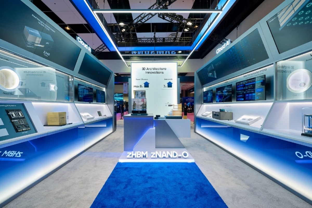
Samsung is showcasing a great variety of memory and storage technologies at its booth at the Future of Memory and Storage (FMS) 2026 event in Santa Clara, California.
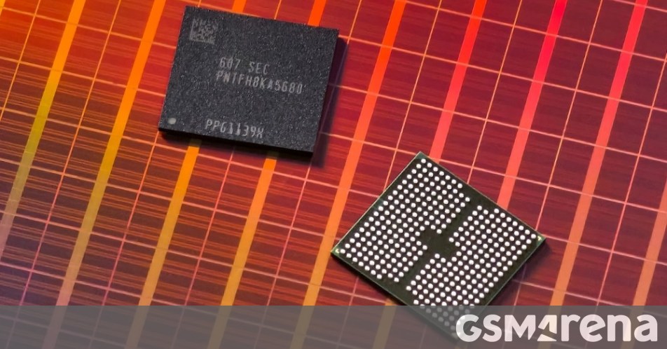
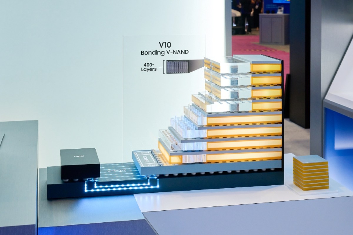
Thirteen years after it introduced the first V-NAND technology, Samsung is the first to unveil V10 of BV-NAND (Bonded V-NAND). This is a flash memory that has more than 400 layers and leverages Samsung’s advanced bonding technology to stack memory cells.
V10 increases memory density by around 58% compared to the previous V9. The higher layer count gives V10 better read, write and I/O performance. It also improves power efficiency.
Samsung started shipping HBM4E samples to customers a few months ago and it also presented HBM5 at FMS, which is the next major industry standard for High Bandwidth Memory (HBM).
However, Samsung also has a proprietary solution called zHBM, which promises approximately eight times the performance of HBM5. This too relies on Samsung’s wafer bonding expertise and can achieve 10x the memory density of HBM5 while tripling the energy efficiency.
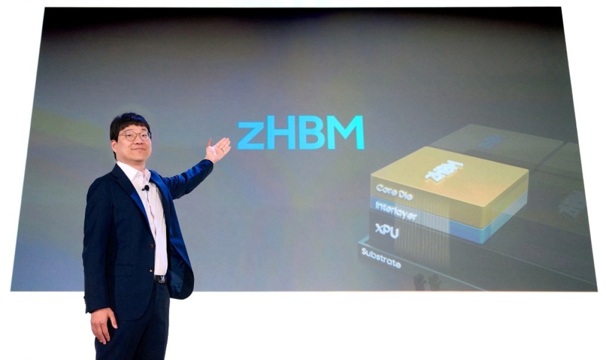
zHBM is designed to stack on top of AI accelerators instead of being placed alongside them on the board. This minimizes the distance that data signals need to travel, which is what enables the higher speeds and superior energy efficiency.
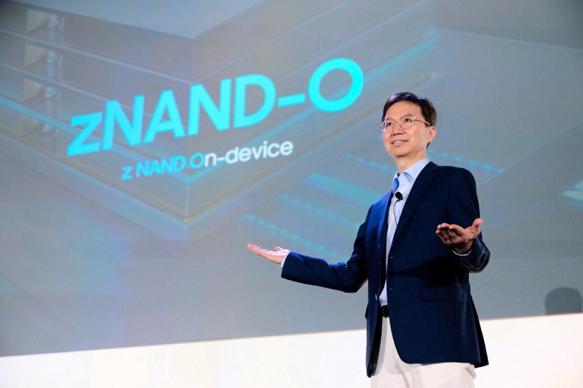
Samsung also introduced zNAND-O, a next-generation flash memory built on its V-NAND technology. It is developing 4 and 8 layer versions and promises high space efficiency, improved I/O performance and lower latency compared to typical NAND storage. zNAND-O is aimed at edge AI (closer to the user), while zHBM is intended for AI training and inference in the cloud.
Additionally, Samsung showcased LPDDR5X-PIM, the industry’s first LPDDR RAM with Processing-In-Memory (PIM). This does some of the data processing within the memory itself before sending the results to the processor. This improves both bandwidth and power efficiency.
The keynote presentation during the opening was titled “Driving the Wave of AI Revolution: 3D Innovations in Memory & Storage Architecture” and was presented by Jin-Yub Lee, Executive Vice President and Head of Flash Product & Technology, and Kyungryun Kim, Vice President and Project Leader of the DRAM Design Team. The keynote laid out Samsung’s ideas on how to maximize AI system performance and power efficiency.